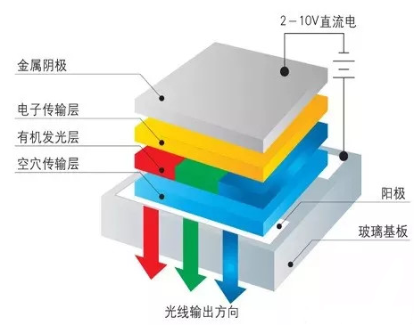
OLED is the abbreviation of Organic Light Emitting Diode,which means “Organic Light Emitting display technology” in Chinese.The idea is that an organic light-emitting layer is sandwiched between two electrodes. When positive and negative electrons meet in the organic material,they emit light. The basic structure of OLED is to make a layer of organic light-emitting material tens of nanometers thick on indium tin oxide (ITO) glass as a light-emitting layer. Above the light-emitting layer is a layer of metal electrodes with low work function, forming a structure like sandwich.

high technology OLED display
Substrate (transparent plastic, glass, foil) – The substrate is used to support the entire OLED.
Anode (TRANSPARENT) – The anode eliminates electrons (increases electron “holes”) as current flows through the device.
Hole transport layer – This layer is made up of organic material molecules that transport “holes” from the anode.
Luminescent layer – This layer is made up of organic material molecules (as opposed to conductive layers) where the luminescence process takes place.
Electron transport layer – This layer is made up of organic material molecules that transport electrons from the cathode.
Cathodes (which can be transparent or opaque, depending on the type of OLED) – When current flows through the device, the cathodes inject electrons into the circuit.
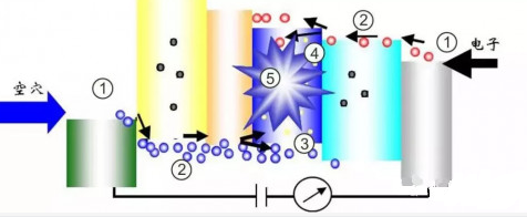
The luminescence process of OLED usually has the following five basic stages:

1. Carrier injection:under the action of an external electric field, electrons and holes are injected into the organic functional layer sandwiched between electrodes from the cathode and anode, respectively.
2. Carrier transport: the injected electrons and holes migrate from the electron transport layer and hole transport layer to the luminescent layer, respectively.
3. Carrier recombination: after the electrons and holes are injected into the luminescent layer, they are bound together to form electron hole pairs, that is, excitons,due to the action of Coulomb force.
4. Exciton migration:Due to the imbalance of electron and hole transport,the main exciton formation region usually does not cover the entire luminescence layer, so diffusion migration will occur due to the concentration gradient.
5. Exciton radiation degenerates photons:An exciton radiative transition that emits photons and releases energy.
Article Source: https://www.disenelec.com/news/what-is-the-oled-display/
Media Contact
Company Name: DISEN ELECTRONICS CO., LTD
Email: Send Email
Country: China
Website: https://www.disenelec.com/


